energy band diagram of pn junction diode pdf
Download Free PDF View PDF. The diode usually consists of a p-n junction which is heavily doped.

Sensors Free Full Text P N Junction Photocurrent Modelling Evaluation Under Optical And Electrical Excitation Html
Download Free PDF View PDF.

. Junction - Contact or connection between two or more wires or cables. The photovoltaic effect is closely related to the photoelectric effectFor both phenomena light is absorbed causing excitation of an electron or other charge carrier to a higher-energy state. ELECTRONICS COMMUNICATION SYSTEM BY GEORGE KENNEDYpdf.
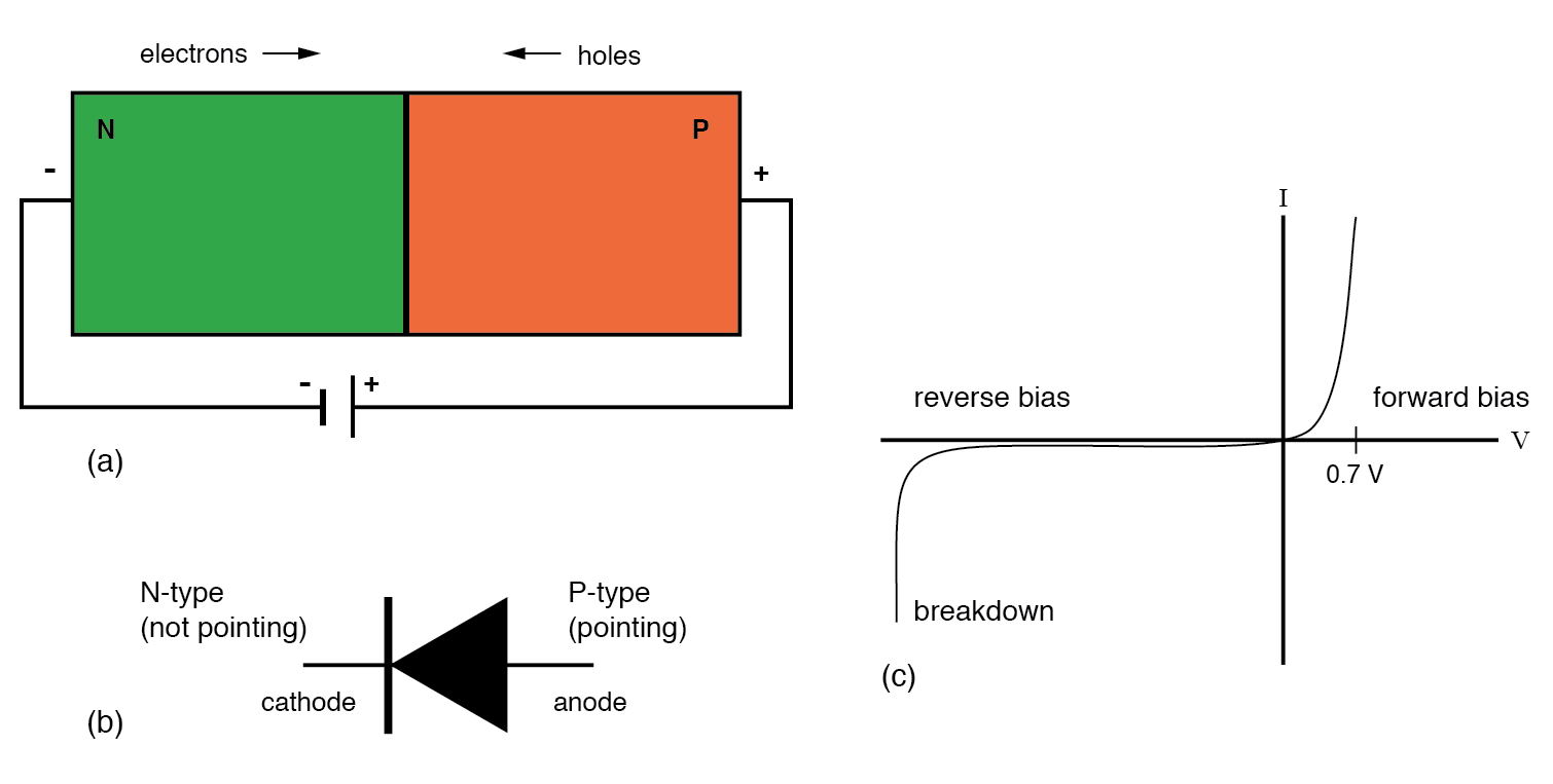
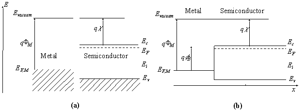
A diode is a two-terminal electronic component that conducts current primarily in one direction asymmetric conductance. Energy states in the bandgap at the metal-semiconductor interface pins Ef to a range of 04 eV to 09 eV below Ec. The depletion area of the diode becomes larger with increasing reverse bias voltage.
The main distinction is that the term. From the diagram we can see that the band around the package corresponds to the line on the diode circuit symbol and this can be an easy way of remembering which end is for which. Keep up with City news services programs events and more.
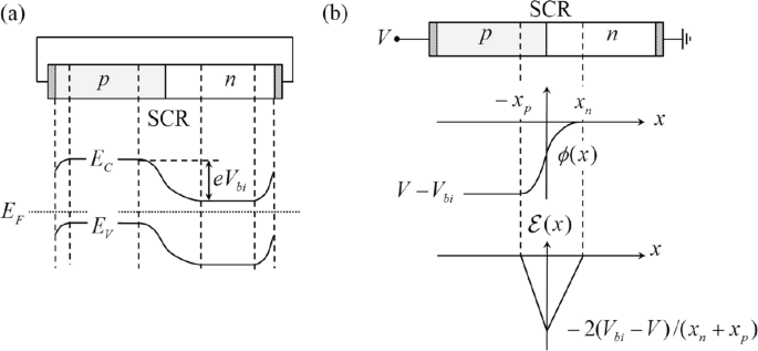
Both p and n junctions are doped at a 1e15 cm -3 160 µCcm 3 doping level leading to built-in potential of 059 V. Download Free PDF View PDF. The lower energy level of a semiconductor is called the valence band E V and the energy level at which an electron can be considered free is called the conduction band E C.
Voltage dependent capacitance of the PN junction. The area where the p-type material and n-type material meet in a semiconductor. I0 of a Schottky diode is 103 to 108 times larger than a PN junction diode depending on.
The band gap E G is the gap in energy between the bound state and the free state between the valence band and conduction band. Temperature is a physical quantity that expresses the hotness of matter or radiation. A The structure diagram of the MoS 2 GaSe heterojunction gas sensor.
ELECTRONICS COMMUNICATION SYSTEM BY GEORGE KENNEDYpdf. It is a form of photoelectric cell defined as a device whose electrical characteristics such as current voltage or resistance vary when exposed to light. Enter the email address you signed up with and well email you a reset link.
Therefore the band gap is the. Download Free PDF View PDF. The left is the energy band diagram of MoS 2 and GaSe the middle is the energy band diagram of the heterojunction of the two materials under light and the right is the energy band diagram of the heterojunction exposed to.
The Zener diode has a reverse-breakdown voltage at which the diode starts conductivity electric current and remains continuous in the reverse-bias mode. BJT as a diode. The Zener diode circuit symbol places two tags at the end of the bar one in the upward direction and the other in the lower direction as shown in the figure.
C Carrier depletion. This ability to change conductivity with the amount of applied voltage can be used for. Reducing depletion width can be inferred from the shrinking carrier motion across the pn junction which as a consequence reduces electrical.
Zener diodes are manufactured with a great variety of Zener voltages and some are even variable. The photovoltaic effect is the generation of voltage and electric current in a material upon exposure to lightIt is a physical and chemical phenomenon. Recently proposed diverse neuron-inspired hardware based on various emerging nanomaterials has effectively advanced neural networks 16 especially for two-dimensional 2D materials.
Joule - The unit of work and energy. It is not a coincidence that the Silicon bandgap ie the energy separating valence. Individual solar cell devices are often the.
Those that rely solely on purely macroscopic properties and. The Art of Electronics - Horowitz Hill. A diode vacuum tube or thermionic diode is a vacuum tube with two electrodes a heated cathode and a plate in which electrons can flow in only one direction.
2D materials can provide a platform to develop transistor architectures for memory operating MOincluding field-effect transistors FETs tunneling transistors junction transistors. B Sensing mechanism of heterojunction gas sensor. Some Zener diodes have a sharp highly doped pn junction with a low Zener voltage in which case the.
I think it will be helpful for the public. It has low ideally zero resistance in one direction and high ideally infinite resistance in the other. A Zener diode is a special type of diode designed to reliably allow current to flow backwards when a certain set reverse voltage known as the Zener voltage is reached.
Ansys Digital Safety Conference 2022. Those such as the SI scale that are defined in terms of the average translational kinetic energy per freely moving microscopic particle such as atom molecule or electron in a body. GATE 2023 Exam - View all the details of the Graduate Aptitude Test in Engineering 2023 exam such as IIT KGP GATE exam dates application eligibility admit card answer key result cut off counselling question papers etc.
The metaloxidesemiconductor field-effect transistor MOSFET MOS-FET or MOS FET is a type of field-effect transistor FET most commonly fabricated by the controlled oxidation of siliconIt has an insulated gate the voltage of which determines the conductivity of the device. With a type II junction band alignment where the bottom of the conduction and the top of the valence bands reside in different layers an external electric field from the gate can modulate the. Electronic Communication System 4th Edition by Kennedy Davispdf.
CsPbI 3 with P m 3 m cubic symmetry exhibits the lowest bandgap E g 173 eV among the all-inorganic Pb-halide perovskite materials for PVHowever at room temperature the orthorhombic phase with Pnma space group symmetry E g 282 eV is thermodynamically preferred To overcome this phase instability the addition of bromide CsPbI 3x Br x has. Official City of Calgary local government Twitter account. The diode is designed to conduct the flow of current in the reverse direction after reaching a specified voltage.
The panels show energy band diagram electric field and net charge density. Energy Band Diagram of Schottky Contact. Join us for this special virtual event on October 18-19 including presentations on MBSE systems engineering safety embedded software and cyber security.
Junction diode - A semiconductor diode in which the rectifying characteristics occur at a junction between the n-type and p-type semiconductor materials. There are three types of temperature scale. Lightly doped p- and n-type regions abut in the waveguide to form a pn diode.
A solar cell or photovoltaic cell is an electronic device that converts the energy of light directly into electricity by the photovoltaic effect which is a physical and chemical phenomenon. PN Diode IV curves. Multi-junction MJ solar cells are solar cells with multiple pn junctions made of different semiconductor materialsEach materials p-n junction will produce electric current in response to different wavelengths of lightThe use of multiple semiconducting materials allows the absorbance of a broader range of wavelengths improving the cells sunlight to electrical.
Pn Junction Diode Springerlink

P N Junction With Reversed Bias Energy Band Diagram Is Also Shown Download Scientific Diagram

Biasing Of P N Junctions

Electronic Devices Energy Band Diagrams In Pn Junction With Fermi Levels Youtube

Semiconductor Physics Energy Band Diagram Of Forward Biased Pn Junction Physics Stack Exchange

Energy Band Diagram An Overview Sciencedirect Topics
The P N Junction Solid State Device Theory Electronics Textbook
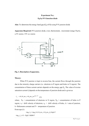
Find Out Band Gap Of Pn Junction Diode Experiment No Eg By P N Junction Diode Aim To Determine Studocu
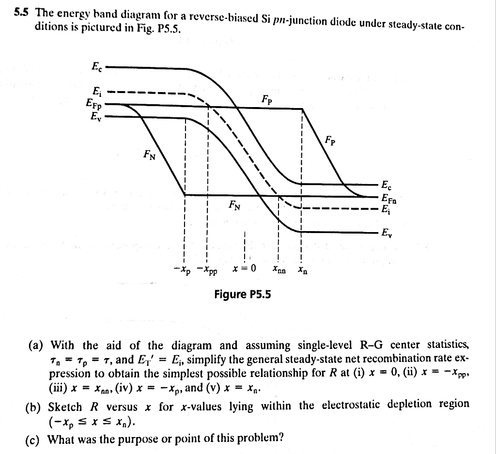
5 5 The Energy Band Diagram For A Reverse Biased Si Chegg Com

Band Diagram Wikiwand
Understanding The Second Approximation Of Diodes Physics Forums
Schottky Diode
2 2 4 Simple Junctions And Devices

4 3 Electrostatic Analysis

Multifunctional Black Phosphorus Mos2 Van Der Waals Heterojunction

4 2 Structure And Principle Of Operation

Exp Physics Lab Ii Experiment No 1 Object To Determine The Band Gap In A Semiconductor Using Its P N Junction Diode Apparatus Required P N Course Hero